ESP32 DEVKIT V1: GPIO Reference
A lookup table for the 30‑pin ESP‑WROOM‑32 board: pick a pin without breaking booting or Wi‑Fi.
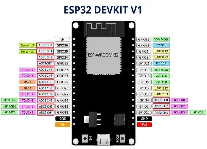
1Quick categories
| Category | Pins | Why |
|---|---|---|
| SAFE general‑purpose | 4, 13, 16, 17, 18, 19, 21, 22, 23, 25, 26, 27, 32, 33 | Use these first for I/O |
| STRAPPING (read at boot) | 0, 2, 5, 12, 15 | Usable, but a wrong level can block uploading |
| BOOT HIGH/PWM | 1, 3, 5, 14, 15 | May glitch attached outputs at reset |
| INPUT‑ONLY | 34, 35, 36 (VP), 39 (VN) | No output, no internal pull |
| DO NOT USE (flash) | 6, 7, 8, 9, 10, 11 | Wired to the SPI flash, not broken out |
| 🔌 USB serial | 1 (TX0), 3 (RX0) | Used by the Serial Monitor: avoid for I/O |
| 🔋 Power in | VIN, 3V3 | VIN feeds the onboard 5V→3.3V regulator; 3V3 is the regulated output |
2Full pin table
I = input · O = output · ADC = analog‑in · Touch = capacitive touch · DAC = analog‑out.
| GPIO | Label | I | O | ADC | Touch | Other | Notes |
|---|---|---|---|---|---|---|---|
| 36 | VP | ✅ | - | ADC1_CH0 | - | Sensor VP | input only |
| 39 | VN | ✅ | - | ADC1_CH3 | - | Sensor VN | input only |
| 34 | D34 | ✅ | - | ADC1_CH6 | - | - | input only |
| 35 | D35 | ✅ | - | ADC1_CH7 | - | - | input only |
| 32 | D32 | ✅ | ✅ | ADC1_CH4 | T9 | - | safe |
| 33 | D33 | ✅ | ✅ | ADC1_CH5 | T8 | - | safe |
| 25 | D25 | ✅ | ✅ | ADC2_CH8 | - | DAC1 | safe |
| 26 | D26 | ✅ | ✅ | ADC2_CH9 | - | DAC2 | safe |
| 27 | D27 | ✅ | ✅ | ADC2_CH7 | T7 | - | safe |
| 14 | D14 | ✅ | ✅ | ADC2_CH6 | T6 | HSPI CLK | PWM at boot |
| 12 | D12 | ✅ | ✅ | ADC2_CH5 | T5 | HSPI MISO | strapping boot fails if pulled HIGH |
| 13 | D13 | ✅ | ✅ | ADC2_CH4 | T4 | HSPI MOSI | safe |
| 23 | D23 | ✅ | ✅ | - | - | VSPI MOSI | safe |
| 22 | D22 | ✅ | ✅ | - | - | I²C SCL | safe |
| 21 | D21 | ✅ | ✅ | - | - | I²C SDA | safe |
| 19 | D19 | ✅ | ✅ | - | - | VSPI MISO | safe |
| 18 | D18 | ✅ | ✅ | - | - | VSPI CLK | safe |
| 5 | D5 | ✅ | ✅ | - | - | VSPI CS | strapping HIGH at boot; PWM at boot |
| 17 | TX2 | ✅ | ✅ | - | - | UART2 TX | safe |
| 16 | RX2 | ✅ | ✅ | - | - | UART2 RX | safe |
| 4 | D4 | ✅ | ✅ | ADC2_CH0 | T0 | - | safe |
| 2 | D2 | ✅ | ✅ | ADC2_CH2 | T2 | On‑board LED | strapping floating/LOW to flash |
| 15 | D15 | ✅ | ✅ | ADC2_CH3 | T3 | HSPI CS | strapping HIGH at boot; PWM at boot |
| 1 | TX0 | - | ✅ | - | - | UART0 TX | Debug output at boot: avoid |
| 3 | RX0 | ✅ | - | - | - | UART0 RX | HIGH at boot: avoid |
| 0 | (BOOT) | ✅ | ✅ | ADC2_CH1 | T1 | Boot select | strapping tied to BOOT; not on header |
3Peripheral defaults
| Bus | Signal → pin |
|---|---|
| I²C | SDA = GPIO 21, SCL = GPIO 22 (reassignable in code) |
| SPI: VSPI | MOSI 23 · MISO 19 · CLK 18 · CS 5 |
| SPI: HSPI | MOSI 13 · MISO 12 · CLK 14 · CS 15 |
| UART0 (USB Serial) | TX 1 · RX 3 |
| UART2 | TX 17 · RX 16 |
| DAC (analog out) | DAC1 = 25 · DAC2 = 26 |
4ADC (analog input) channels
ADC is 12‑bit → readings 0–4095 for 0–3.3 V.
- ADC1 (always usable): GPIO 32, 33, 34, 35, 36, 39
- ADC2 (⚠️ unusable while Wi‑Fi is on): GPIO 0, 2, 4, 12, 13, 14, 15, 25, 26, 27
5Capacitive touch channels
Touch T0–T9: T0=4, T1=0, T2=2, T3=15, T4=13, T5=12, T6=14, T7=27, T8=33, T9=32.
6Electrical limits
- ≤ 40 mA per GPIO absolute; keep ≤ ~12 mA in practice.
- Logic is 3.3 V: never apply 5 V to a GPIO.
- Input‑only pins (34/35/36/39) have no internal pull: add an external resistor for buttons.
7VIN pin (external 5V power input)
VIN feeds the board's onboard AMS1117 5V→3.3V linear regulator, which in turn powers the ESP32 chip via the 3V3 pin. It's how you power the board without USB — e.g. from a battery pack or bench supply.
- Accepted range: roughly 4.5–12 V (the AMS1117's dropout voltage is ~1.1–1.3 V, so it needs at least ~4.5 V in to reliably output a clean 3.3 V).
- Recommended: 6–7 V — high enough for headroom, low enough that the regulator doesn't waste much power as heat.
- Absolute ceiling: avoid going above 12 V; the linear regulator dissipates the difference as heat and can overheat/shut down or fail at higher voltages, especially under load.
- On many DEVKIT V1 boards, VIN and 5V are the same net — check your specific board's silkscreen/schematic before assuming.
- VIN is bidirectional, not just an input. It's a plain wire to that shared 5V net, with no diode or switch enforcing a direction. Power the board over USB with nothing plugged into VIN, and USB's 5 V flows out through that same net, making VIN a 5 V power source you can tap for accessories, e.g. the HC‑SR501 PIR sensor's VCC in Project 4. Feed an external supply into VIN instead, and current flows the other way, into the regulator. Never do both at once: two live 5 V sources on one net will fight each other.
- Never apply reverse polarity or exceed the ceiling: there's no onboard reverse-protection on many clones.
More: ESP32 pinout reference (Random Nerd Tutorials) → · DOIT ESP32 DEVKIT V1 specs (espboards.dev) →
🎯 Knowledge Check
1. Which GPIO pins should NEVER be used because they are wired to the internal SPI flash?
2. Which ADC bank stops working when Wi-Fi is active?
3. What is the maximum safe current per GPIO pin?
4. Which pins are input-only and have no internal pull-up or pull-down?
Ask about wiring, code, or troubleshooting for any project in this kit.